Skip to content
Centre for III-nitride technology
Centre for III-nitride technology
Home
Goals
Projects
News and Events
Publications
Partners
Center Organization
Accessibility
Contact
Search for:
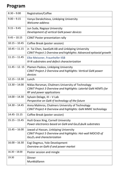
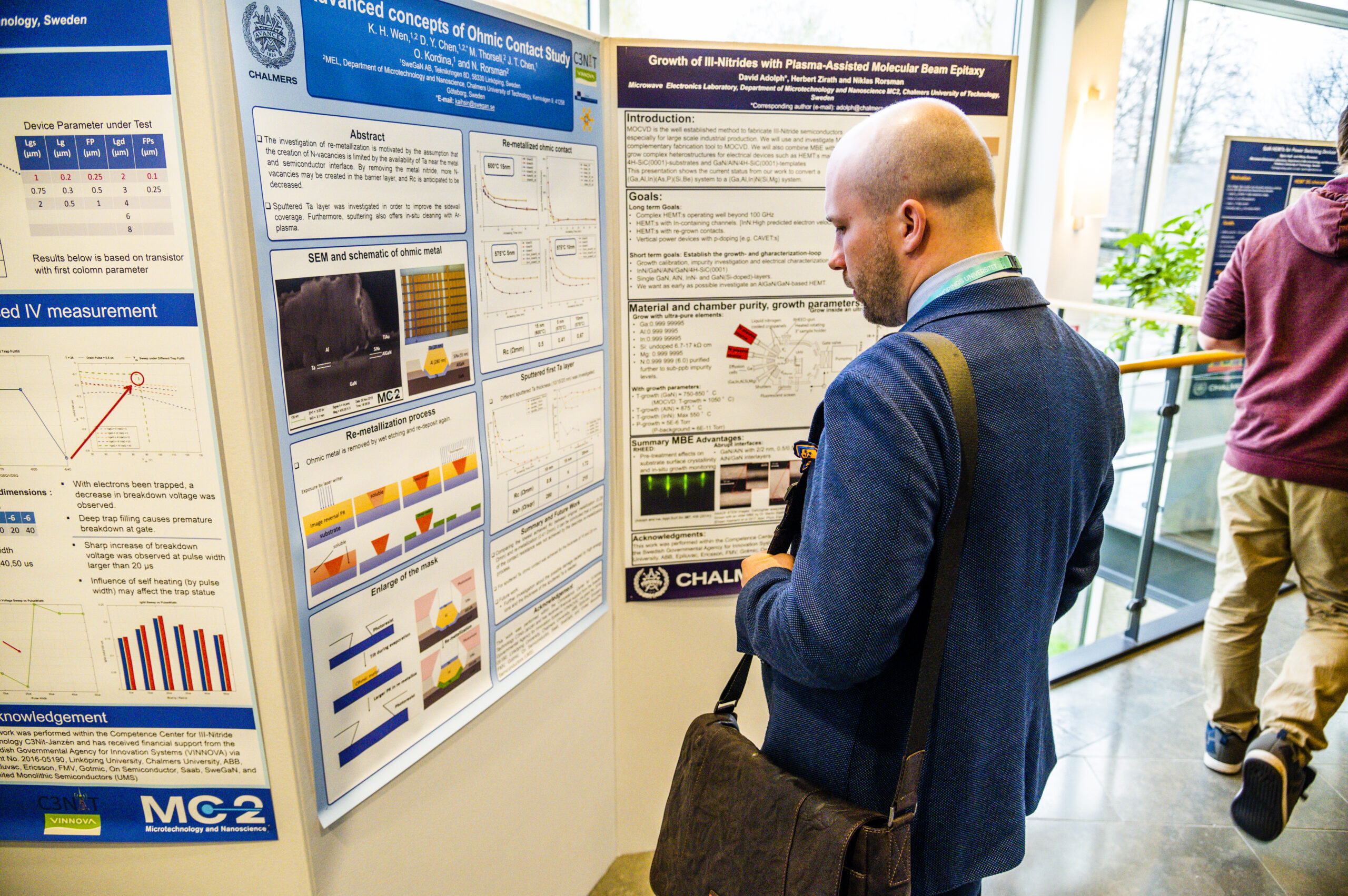
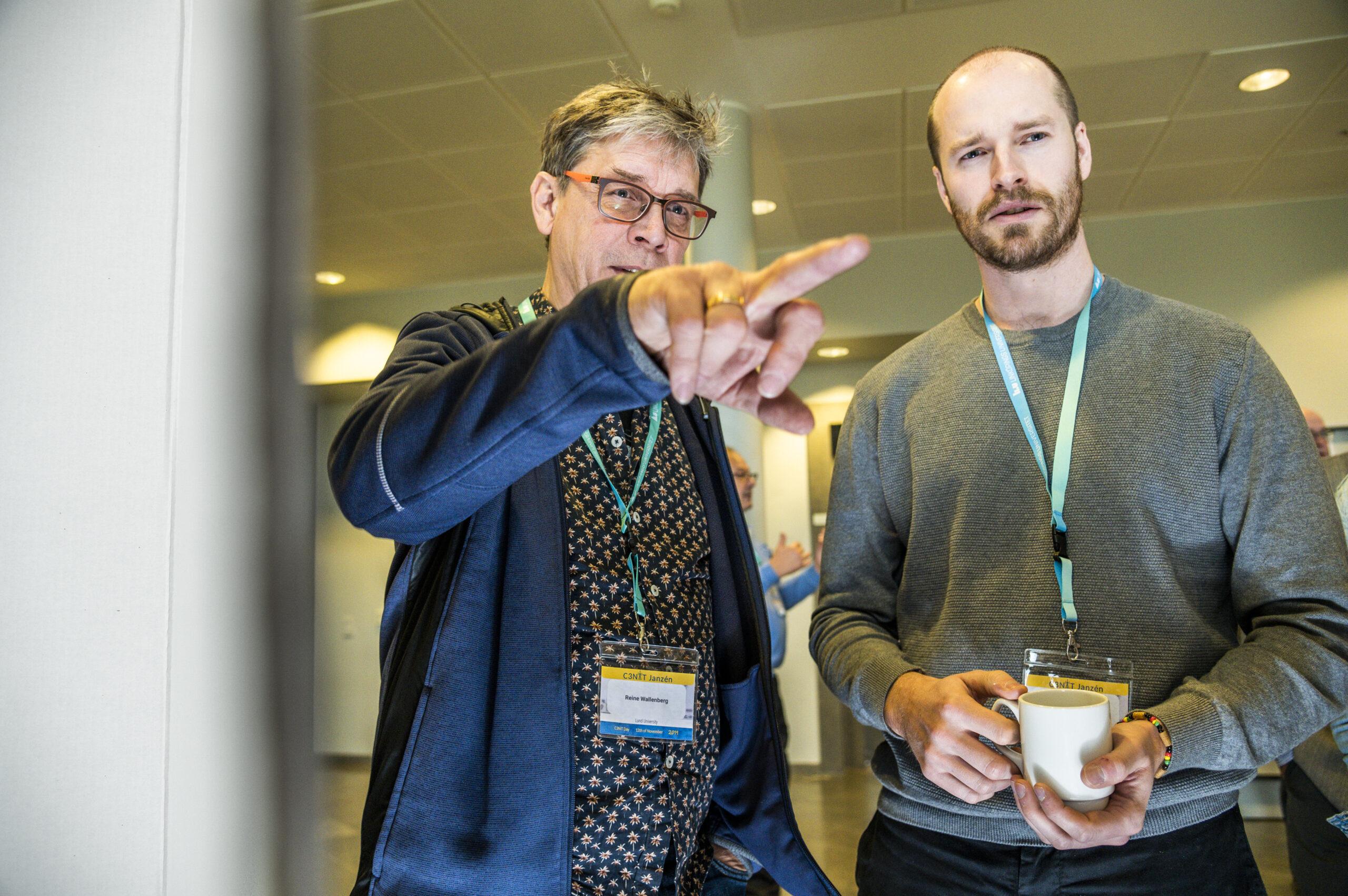
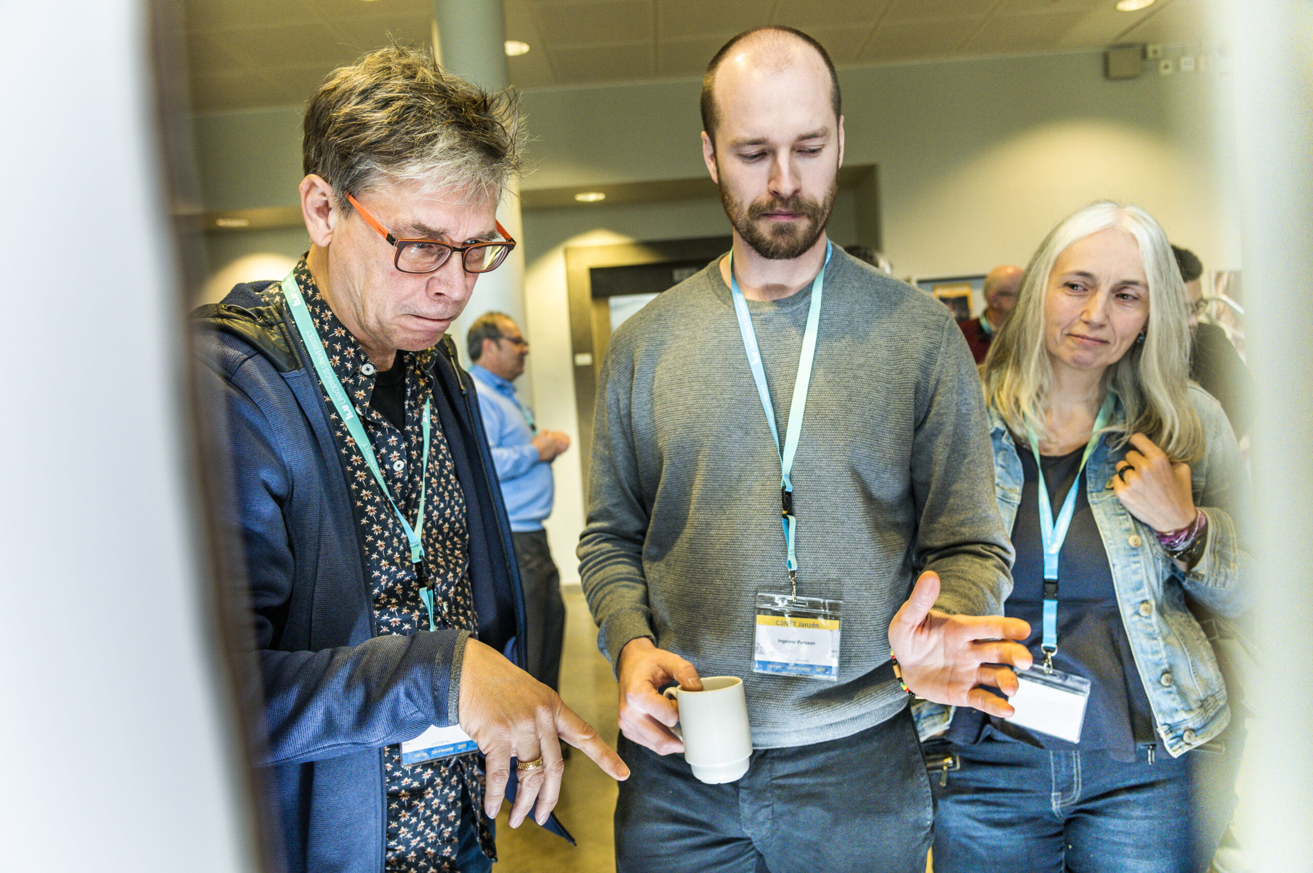
C3NiT day 2019
Home
/
C3NiT days
/
C3NiT day 2019
C3NiT day 2019
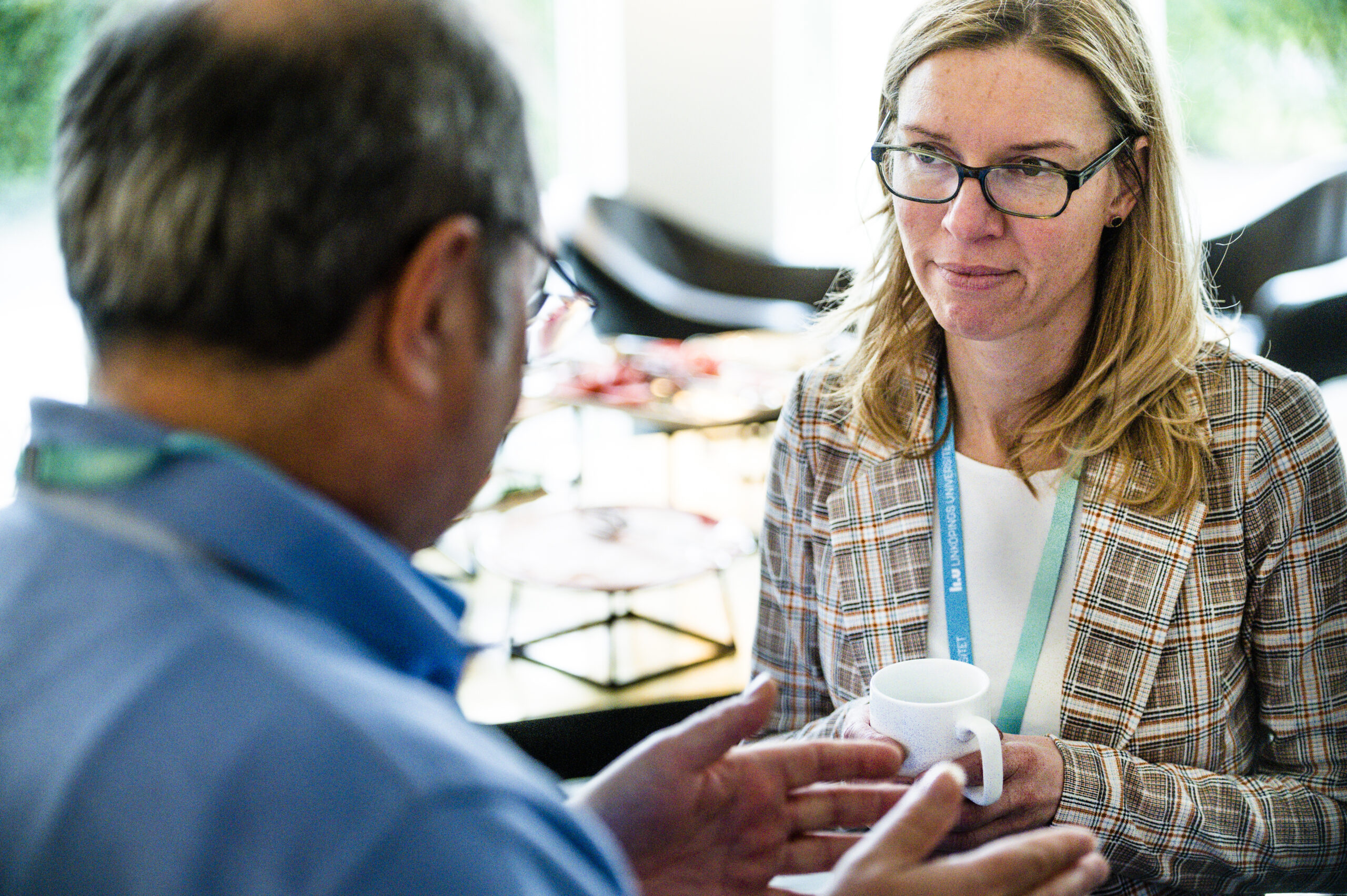
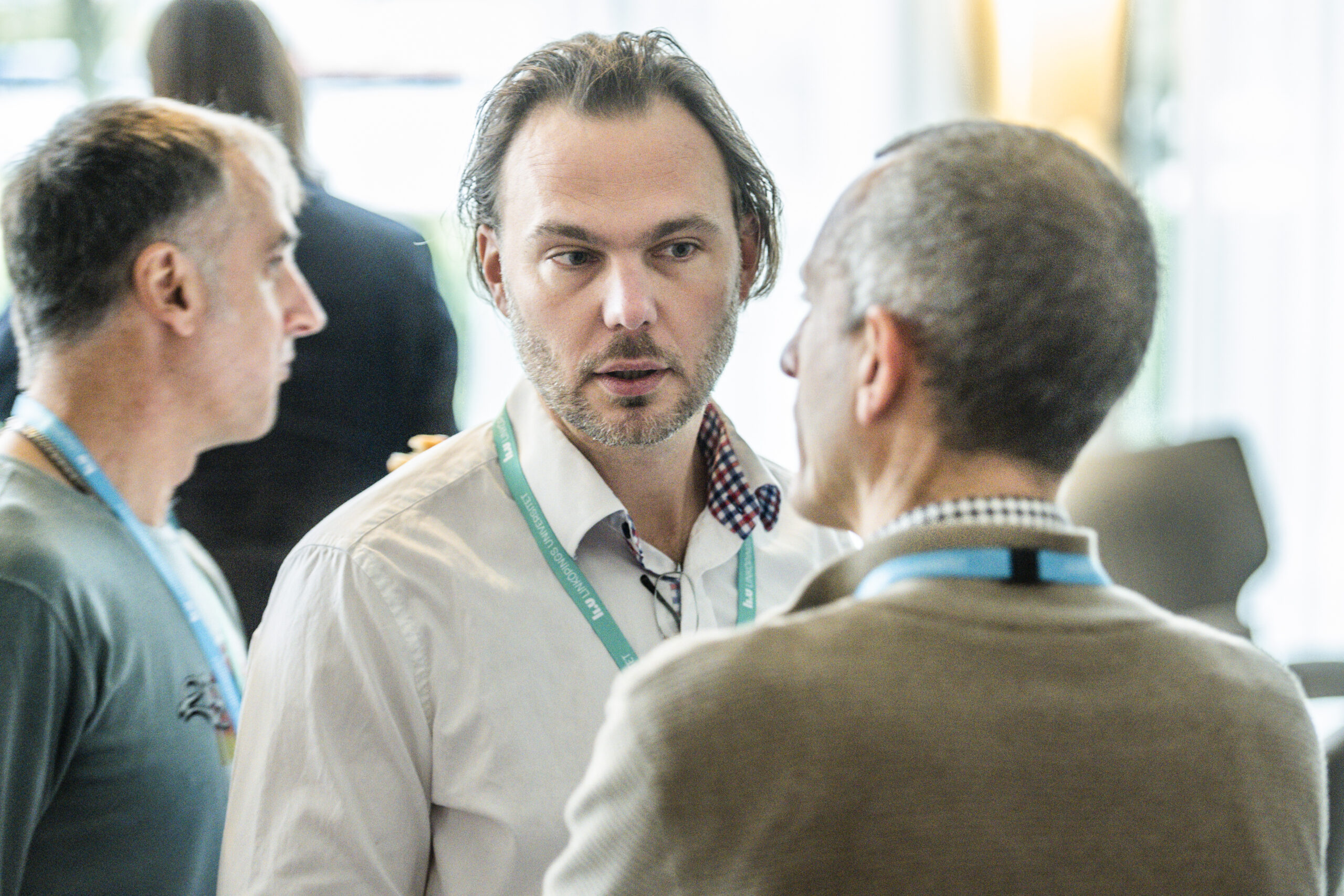
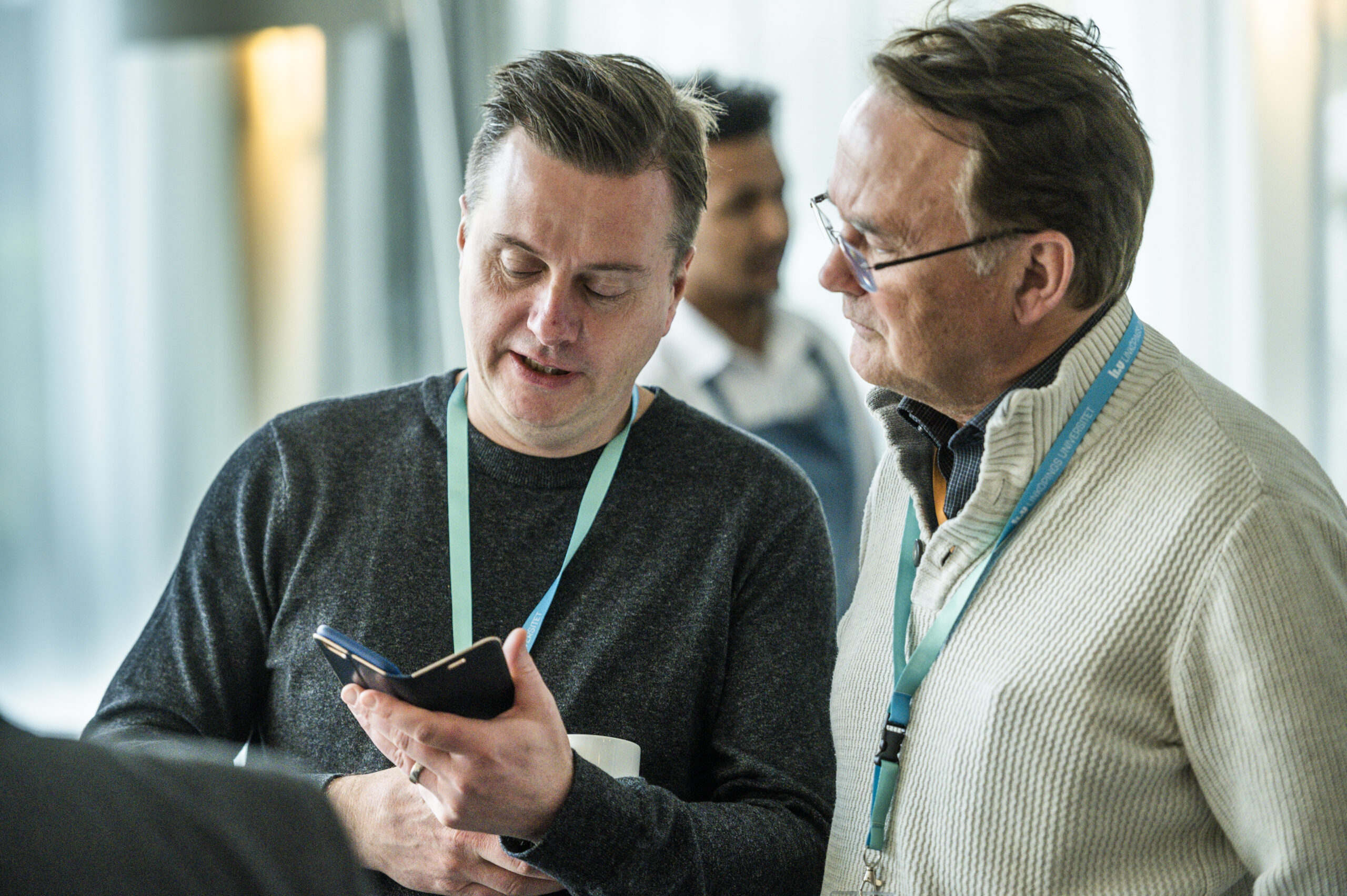
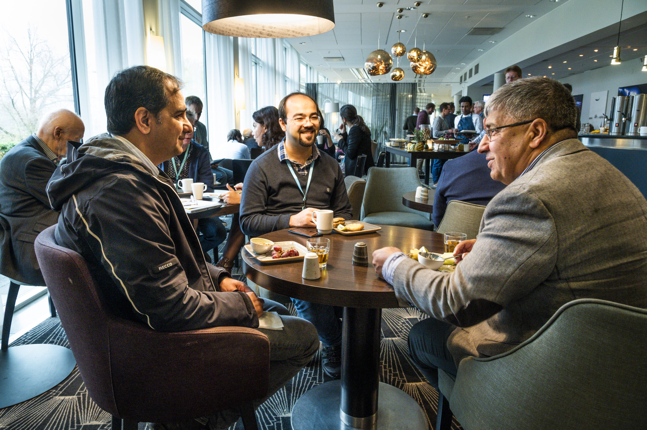
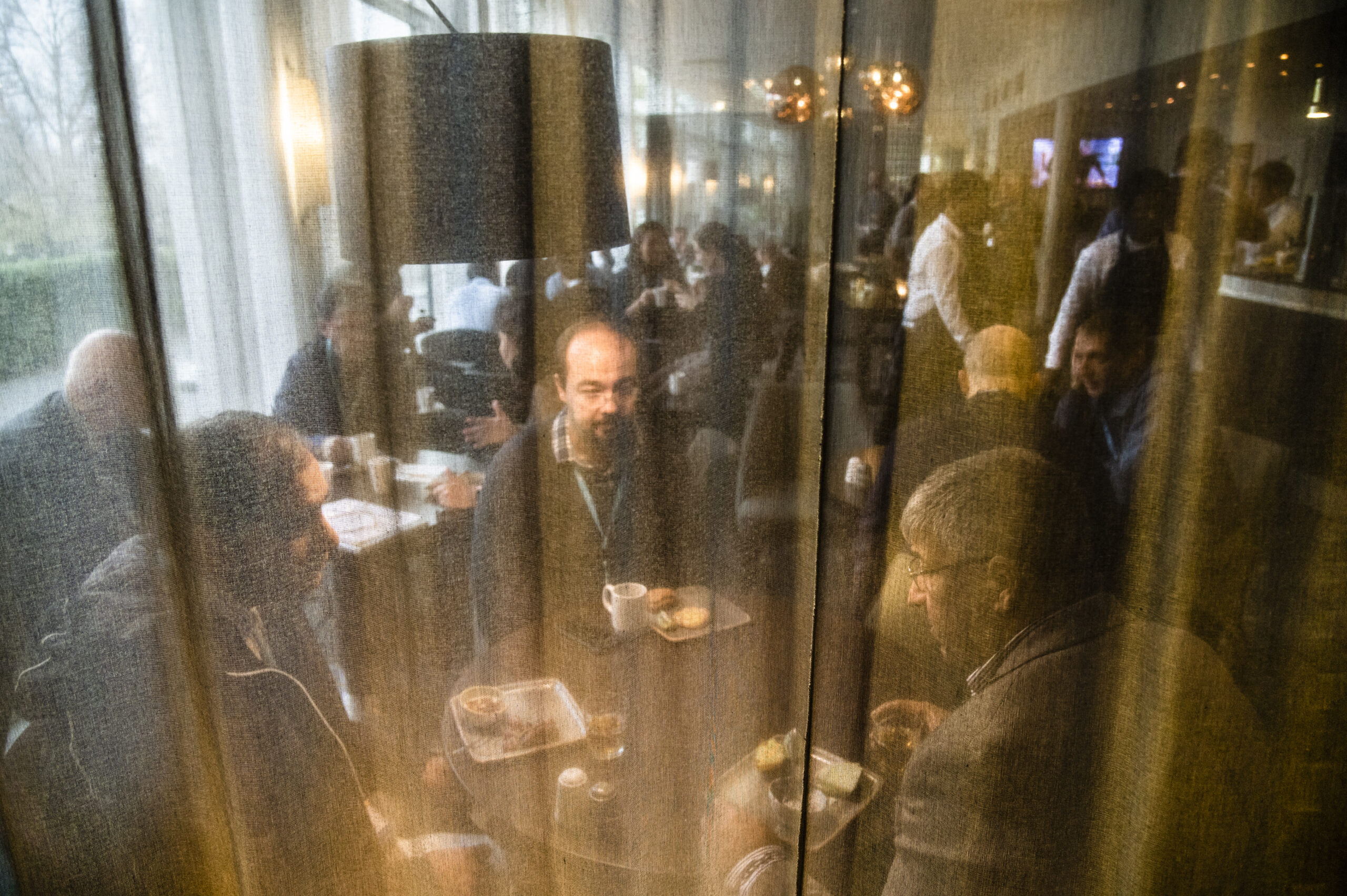
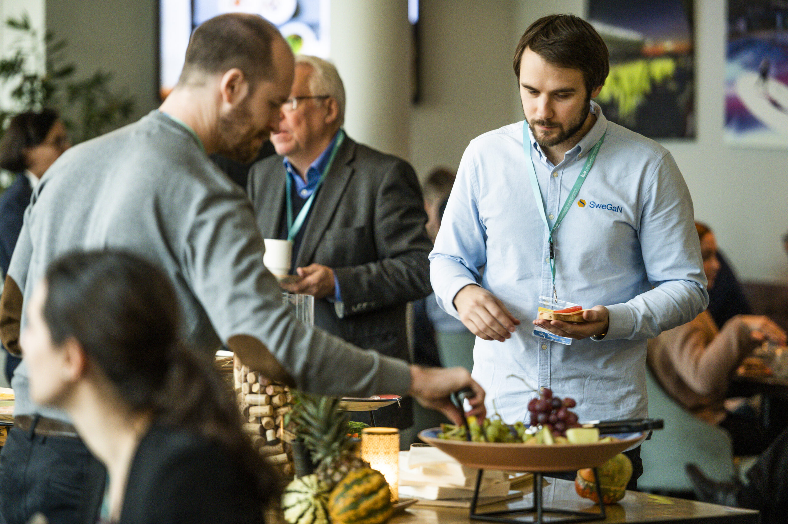
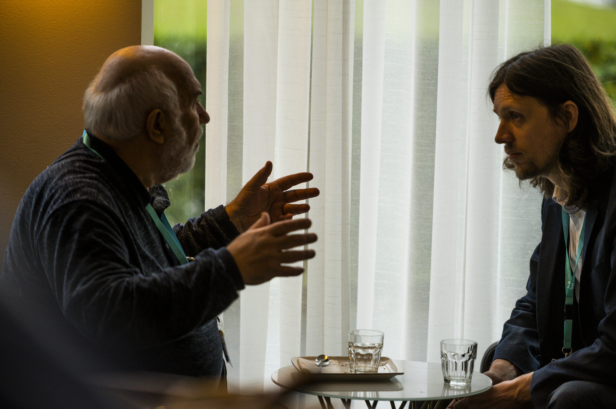
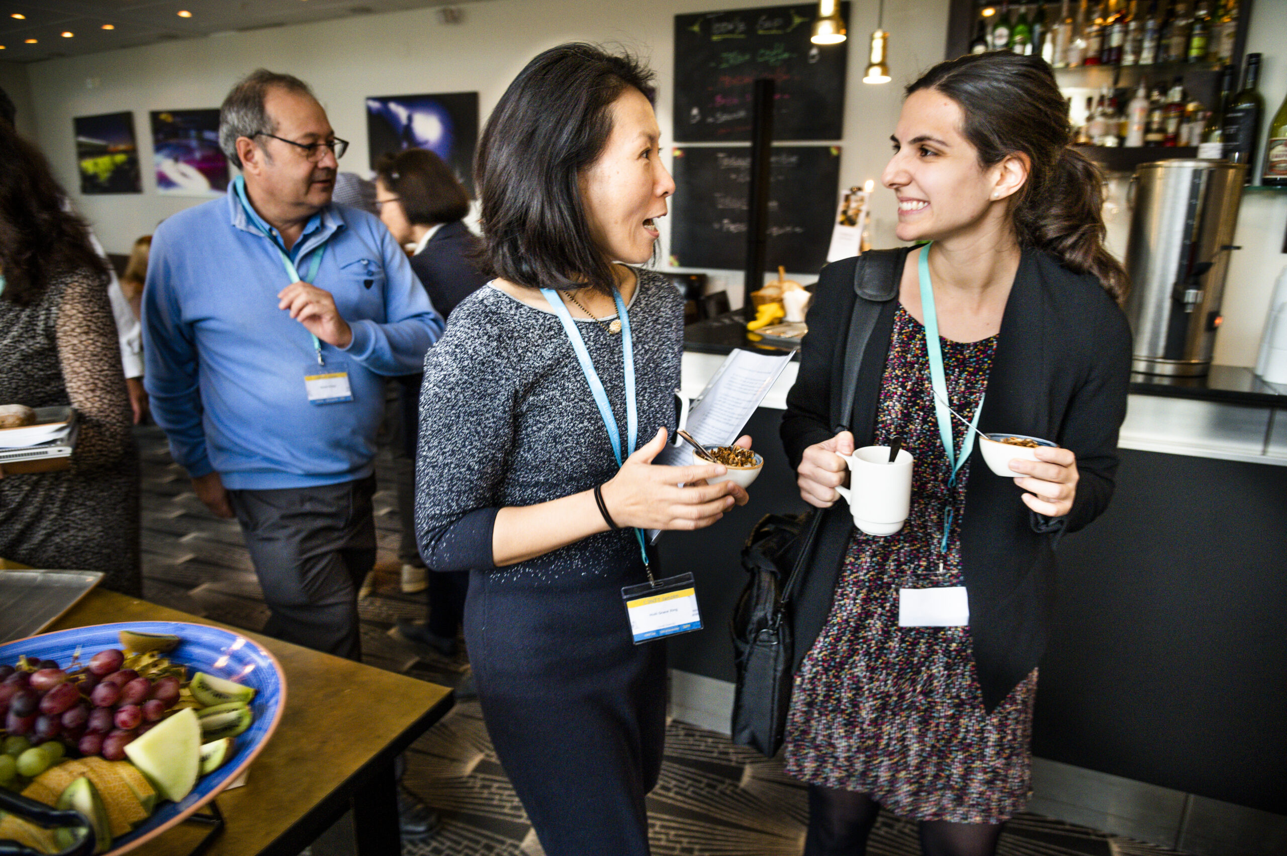
Photo Gallery C3NiT day 2019
Copyright © 2025 C3NiT -Janzén | A Vinnova Competence Centre